Introduction
In this tutorial, you will learn all about the I2C communication protocol, why you would want to use it, and how it’s implemented.
The Inter-integrated Circuit (I2C) Protocol is a protocol intended to allow multiple “slave” digital integrated circuits (“chips”) to communicate with one or more “master” chips. Like the Serial Peripheral Interface (SPI), it is only intended for short distance communications within a single device. Like Asynchronous Serial Interfaces (such as RS-232 or UARTs), it only requires two signal wires to exchange information.
Why Use I2C?
To figure out why one might want to communicate over I2C, you must first compare it to the other available options to see how it differs.
To figure out why one might want to communicate over I2C, you must first compare it to the other available options to see how it differs.
Enter I2C – The Best of Both Worlds!
 I2C requires a mere two wires, like asynchronous serial, but those two wires can support up to 1008 slave devices. Also, unlike SPI, I2C can support a multi-master system, allowing more than one master to communicate with all devices on the bus (although the master devices can’t talk to each other over the bus and must take turns using the bus lines).
Data rates fall between asynchronous serial and SPI; most I2C devices can communicate at 100kHz or 400kHz. There is some overhead with I2C; for every 8 bits of data to be sent, one extra bit of meta data (the “ACK/NACK” bit, which we’ll discuss later) must be transmitted.
The hardware required to implement I2C is more complex than SPI, but less than asynchronous serial. It can be fairly trivially implemented in software.
I2C requires a mere two wires, like asynchronous serial, but those two wires can support up to 1008 slave devices. Also, unlike SPI, I2C can support a multi-master system, allowing more than one master to communicate with all devices on the bus (although the master devices can’t talk to each other over the bus and must take turns using the bus lines).
Data rates fall between asynchronous serial and SPI; most I2C devices can communicate at 100kHz or 400kHz. There is some overhead with I2C; for every 8 bits of data to be sent, one extra bit of meta data (the “ACK/NACK” bit, which we’ll discuss later) must be transmitted.
The hardware required to implement I2C is more complex than SPI, but less than asynchronous serial. It can be fairly trivially implemented in software.
I2C – A Brief History
I2C was originally developed in 1982 by Philips for various Philips chips. The original spec allowed for only 100kHz communications, and provided only for 7-bit addresses, limiting the number of devices on the bus to 112 (there are several reserved addresses, which will never be used for valid I2C addresses). In 1992, the first public specification was published, adding a 400kHz fast-mode as well as an expanded 10-bit address space. Much of the time (for instance, in the ATMega328 device on many Arduino-compatible boards) , device support for I2C ends at this point. There are three additional modes specified: fast-mode plus, at 1MHz; high-speed mode, at 3.4MHz; and ultra-fast mode, at 5MHz.
In addition to “vanilla” I2C, Intel introduced a variant in 1995 call “System Management Bus” (SMBus). SMBus is a more tightly controlled format, intended to maximize predictability of communications between support ICs on PC motherboards. The most significant difference between SMBus is that it limits speeds from 10kHz to 100kHz, while I2C can support devices from 0kHz to 5MHz. SMBus includes a clock timeout mode which makes low-speed operations illegal, although many SMBus devices will support it anyway to maximize interoperability with embedded I2C systems.
I2C at the Hardware Level
Signals
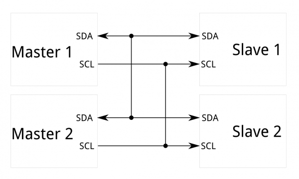
Each I2C bus consists of two signals: SCL and SDA. SCL is the clock signal, and SDA is the data signal. The clock signal is always generated by the current bus master; some slave devices may force the clock low at times to delay the master sending more data (or to require more time to prepare data before the master attempts to clock it out). This is called “clock stretching” and is described on the protocol page.
Unlike UART or SPI connections, the I2C bus drivers are “open drain”, meaning that they can pull the corresponding signal line low, but cannot drive it high. Thus, there can be no bus contention where one device is trying to drive the line high while another tries to pull it low, eliminating the potential for damage to the drivers or excessive power dissipation in the system. Each signal line has a pull-up resistor on it, to restore the signal to high when no device is asserting it low.
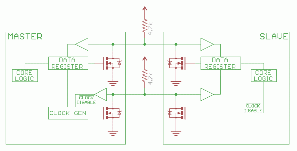 Notice the two pull-up resistors on the two communication lines.
Resistor selection varies with devices on the bus, but a good rule of thumb is to start with 4.7k and adjust down if necessary. I2C is a fairly robust protocol, and can be used with short runs of wire (2-3m). For long runs, or systems with lots of devices, smaller resistors are better.
Notice the two pull-up resistors on the two communication lines.
Resistor selection varies with devices on the bus, but a good rule of thumb is to start with 4.7k and adjust down if necessary. I2C is a fairly robust protocol, and can be used with short runs of wire (2-3m). For long runs, or systems with lots of devices, smaller resistors are better.
Each I2C bus consists of two signals: SCL and SDA. SCL is the clock signal, and SDA is the data signal. The clock signal is always generated by the current bus master; some slave devices may force the clock low at times to delay the master sending more data (or to require more time to prepare data before the master attempts to clock it out). This is called “clock stretching” and is described on the protocol page.
Unlike UART or SPI connections, the I2C bus drivers are “open drain”, meaning that they can pull the corresponding signal line low, but cannot drive it high. Thus, there can be no bus contention where one device is trying to drive the line high while another tries to pull it low, eliminating the potential for damage to the drivers or excessive power dissipation in the system. Each signal line has a pull-up resistor on it, to restore the signal to high when no device is asserting it low.
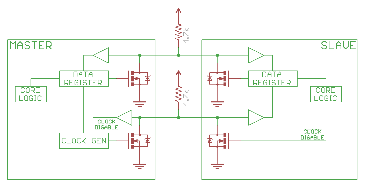
Notice the two pull-up resistors on the two communication lines.
Resistor selection varies with devices on the bus, but a good rule of thumb is to start with 4.7k and adjust down if necessary. I2C is a fairly robust protocol, and can be used with short runs of wire (2-3m). For long runs, or systems with lots of devices, smaller resistors are better.
Signal Levels
Since the devices on the bus don’t actually drive the signals high, I2C allows for some flexibility in connecting devices with different I/O voltages. In general, in a system where one device is at a higher voltage than another, it may be possible to connect the two devices via I2C without any level shifting circuitry in between them. The trick is to connect the pull-up resistors to the lower of the two voltages. This only works in some cases, where the lower of the two system voltages exceeds the high-level input voltage of the the higher voltage system–for example, a 5V Arduino and a 3.3V accelerometer.
If the voltage difference between the two systems is too great (say, 5V and 2.5V), SparkFun offers a simple I2C level shifter board. Since the board also includes an enable line, it can be used to disable communications to selected devices. This is useful in cases where more than one device with the same address is to be connected to a single master–Wii Nunchucks are a good example.
Protocol
Communication via I2C is more complex than with a UART or SPI solution. The signalling must adhere to a certain protocol for the devices on the bus to recognize it as valid I2C communications. Fortunately, most devices take care of all the fiddly details for you, allowing you to concentrate on the data you wish to exchange.
Communication via I2C is more complex than with a UART or SPI solution. The signalling must adhere to a certain protocol for the devices on the bus to recognize it as valid I2C communications. Fortunately, most devices take care of all the fiddly details for you, allowing you to concentrate on the data you wish to exchange.
Basics
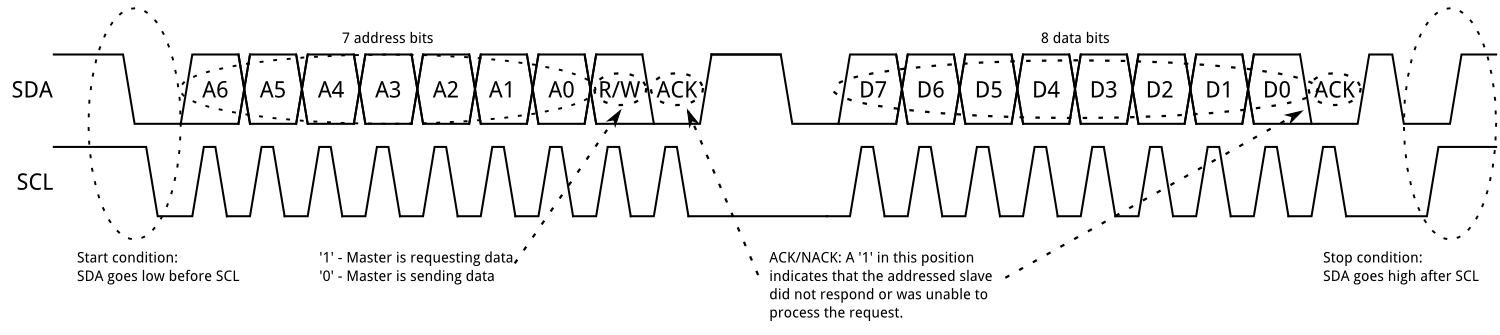
 Messages are broken up into two types of frame: an address frame, where the master indicates the slave to which the message is being sent, and one or more data frames, which are 8-bit data messages passed from master to slave or vice versa. Data is placed on the SDA line after SCL goes low, and is sampled after the SCL line goes high. The time between clock edge and data read/write is defined by the devices on the bus and will vary from chip to chip.
Messages are broken up into two types of frame: an address frame, where the master indicates the slave to which the message is being sent, and one or more data frames, which are 8-bit data messages passed from master to slave or vice versa. Data is placed on the SDA line after SCL goes low, and is sampled after the SCL line goes high. The time between clock edge and data read/write is defined by the devices on the bus and will vary from chip to chip.
Start Condition
To initiate the address frame, the master device leaves SCL high and pulls SDA low. This puts all slave devices on notice that a transmission is about to start. If two master devices wish to take ownership of the bus at one time, whichever device pulls SDA low first wins the race and gains control of the bus. It is possible to issue repeated starts, initiating a new communication sequence without relinquishing control of the bus to other masters; we’ll talk about that later.
To initiate the address frame, the master device leaves SCL high and pulls SDA low. This puts all slave devices on notice that a transmission is about to start. If two master devices wish to take ownership of the bus at one time, whichever device pulls SDA low first wins the race and gains control of the bus. It is possible to issue repeated starts, initiating a new communication sequence without relinquishing control of the bus to other masters; we’ll talk about that later.
Address Frame
The address frame is always first in any new communication sequence. For a 7-bit address, the address is clocked out most significant bit (MSB) first, followed by a R/W bit indicating whether this is a read (1) or write (0) operation.
The 9th bit of the frame is the NACK/ACK bit. This is the case for all frames (data or address). Once the first 8 bits of the frame are sent, the receiving device is given control over SDA. If the receiving device does not pull the SDA line low before the 9th clock pulse, it can be inferred that the receiving device either did not receive the data or did not know how to parse the message. In that case, the exchange halts, and it’s up to the master of the system to decide how to proceed.
Data Frames
After the address frame has been sent, data can begin being transmitted. The master will simply continue generating clock pulses at a regular interval, and the data will be placed on SDA by either the master or the slave, depending on whether the R/W bit indicated a read or write operation. The number of data frames is arbitrary, and most slave devices will auto-increment the internal register, meaning that subsequent reads or writes will come from the next register in line.
After the address frame has been sent, data can begin being transmitted. The master will simply continue generating clock pulses at a regular interval, and the data will be placed on SDA by either the master or the slave, depending on whether the R/W bit indicated a read or write operation. The number of data frames is arbitrary, and most slave devices will auto-increment the internal register, meaning that subsequent reads or writes will come from the next register in line.
Stop condition
Once all the data frames have been sent, the master will generate a stop condition. Stop conditions are defined by a 0->1 (low to high) transition on SDA after a 0->1 transition on SCL, with SCL remaining high. During normal data writing operation, the value on SDA should not change when SCL is high, to avoid false stop conditions.
Once all the data frames have been sent, the master will generate a stop condition. Stop conditions are defined by a 0->1 (low to high) transition on SDA after a 0->1 transition on SCL, with SCL remaining high. During normal data writing operation, the value on SDA should not change when SCL is high, to avoid false stop conditions.
Advanced Protocol Topics
10-bit Addresses
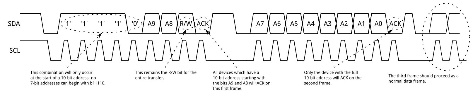
 In a 10-bit addressing system, two frames are required to transmit the slave address. The first frame will consist of the code b11110xyz, where ‘x’ is the MSB of the slave address, y is bit 8 of the slave address, and z is the read/write bit as described above. The first frame’s ACK bit will be asserted by all slaves which match the first two bits of the address. As with a normal 7-bit transfer, another transfer begins immediately, and this transfer contains bits 7:0 of the address. At this point, the addressed slave should respond with an ACK bit. If it doesn’t, the failure mode is the same as a 7-bit system.
Note that 10-bit address devices can coexist with 7-bit address devices, since the leading ‘11110’ part of the address is not a part of any valid 7-bit addresses.
In a 10-bit addressing system, two frames are required to transmit the slave address. The first frame will consist of the code b11110xyz, where ‘x’ is the MSB of the slave address, y is bit 8 of the slave address, and z is the read/write bit as described above. The first frame’s ACK bit will be asserted by all slaves which match the first two bits of the address. As with a normal 7-bit transfer, another transfer begins immediately, and this transfer contains bits 7:0 of the address. At this point, the addressed slave should respond with an ACK bit. If it doesn’t, the failure mode is the same as a 7-bit system.
Note that 10-bit address devices can coexist with 7-bit address devices, since the leading ‘11110’ part of the address is not a part of any valid 7-bit addresses.
Repeated Start Conditions
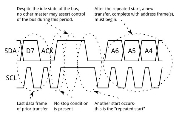 Sometimes, it is important that a master device be allowed to exchange several messages in one go, without allowing other master devices on the bus to interfere. For this reason, the repeated start condition has been defined.
To perform a repeated start, SDA is allowed to go high while SCL is low, SCL is allowed to go high, and then SDA is brought low again while SCL is high. Because there was no stop condition on the bus, the previous communication wasn’t truly completed and the current master maintains control of the bus.
At this point, the next message can begin transmission. The syntax of this new message is the same as any other message–an address frame followed by data frames. Any number of repeated starts is allowed, and the master will maintain control of the bus until it issues a stop condition.
Sometimes, it is important that a master device be allowed to exchange several messages in one go, without allowing other master devices on the bus to interfere. For this reason, the repeated start condition has been defined.
To perform a repeated start, SDA is allowed to go high while SCL is low, SCL is allowed to go high, and then SDA is brought low again while SCL is high. Because there was no stop condition on the bus, the previous communication wasn’t truly completed and the current master maintains control of the bus.
At this point, the next message can begin transmission. The syntax of this new message is the same as any other message–an address frame followed by data frames. Any number of repeated starts is allowed, and the master will maintain control of the bus until it issues a stop condition.
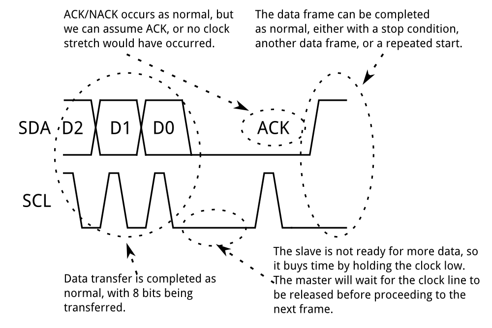
Clock stretching
 At times, the master’s data rate will exceed the slave’s ability to provide that data. This can be because the data isn’t ready yet (for instance, the slave hasn’t completed an analog-to-digital conversion yet) or because a previous operation hasn’t yet completed (say, an EEPROM which hasn’t completed writing to non-volatile memory yet and needs to finish that before it can service other requests).
In this case, some slave devices will execute what is referred to as “clock stretching”. Nominally, all clocking is driven by the master device–slaves simply put data on the bus or take data off the bus in response to the master’s clock pulses. At any point in the data transfer process, an addressed slave can hold the SCL line low after the master releases it. The master is required to refrain from additional clock pulses or data transfer until such time as the slave releases the SCL line.
At times, the master’s data rate will exceed the slave’s ability to provide that data. This can be because the data isn’t ready yet (for instance, the slave hasn’t completed an analog-to-digital conversion yet) or because a previous operation hasn’t yet completed (say, an EEPROM which hasn’t completed writing to non-volatile memory yet and needs to finish that before it can service other requests).
In this case, some slave devices will execute what is referred to as “clock stretching”. Nominally, all clocking is driven by the master device–slaves simply put data on the bus or take data off the bus in response to the master’s clock pulses. At any point in the data transfer process, an addressed slave can hold the SCL line low after the master releases it. The master is required to refrain from additional clock pulses or data transfer until such time as the slave releases the SCL line.
No comments:
Post a Comment