WiFi Module

Introduction
When power is applied to the module you should see the red power light turn on and the blue serial
indicator light flicker briefly.
If you have a 3.3V FTDI Serial to USB board you can get started without fear of destroying your new
ESP8266 WiFi module. Do note that many FTDI boards have a solder jumper to convert from 3.3V to
5V operation so ensure it is set to enable 3.3V operation.
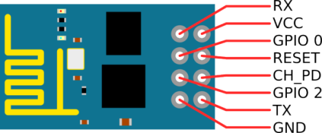
Here are the connections required to enable communication with the module over serial:
What is this ESP8266
- It's a wireless SoC
- It has GPIO, I2C, ADC, SPI, PWM and some more
- It's running at 80MHz
- 64KBytes of instruction RAM
- 96KBytes of data RAM
- 64KBytes boot ROM
- It has a Winbond W25Q40BVNIG SPI flash
- It's a RISC architecture
- The core is a 106micro Diamond Standard core (LX3) made by Tensilica
- The ESP8266 chip is made by Espressif
- Modules bearing this chip are made by various manufacturers
Description:
The ESP8266 WiFi Module is a self contained SOC with integrated TCP/IP protocol stack that can give any microcontroller access to your WiFi network. The ESP8266 is capable of either hosting an application or offloading all Wi-Fi networking functions from another application processor. Each ESP8266 module comes pre-programmed with an AT command set firmware, meaning, you can simply hook this up to your Arduino device and get about as much WiFi-ability as a WiFi Shield offers (and that’s just out of the box)! The ESP8266 module is an extremely cost effective board with a huge, and ever growing, community.
This module has a powerful enough on-board processing and storage capability that allows it to be integrated with the sensors and other application specific devices through its GPIOs with minimal development up-front and minimal loading during runtime. Its high degree of on-chip integration allows for minimal external circuitry, including the front-end module, is designed to occupy minimal PCB area. The ESP8266 supports APSD for VoIP applications and Bluetooth co-existance interfaces, it contains a self-calibrated RF allowing it to work under all operating conditions, and requires no external RF parts.
There is an almost limitless fountain of information available for the ESP8266, all of which has been provided by amazing community support. In the Documents section below you will find many resources to aid you in using the ESP8266, even instructions on how to transforming this module into an IoT (Internet of Things) solution!
Note: The ESP8266 Module is not capable of 5-3V logic shifting and will require an external Logic Level Converter. Please do not power it directly from your 5V dev board.
Note: This new version of the ESP8266 WiFi Module has increased the flash disk size from 512k to 1MB.
Features:
- 802.11 b/g/n
- Wi-Fi Direct (P2P), soft-AP
- Integrated TCP/IP protocol stack
- Integrated TR switch, balun, LNA, power amplifier and matching network
- Integrated PLLs, regulators, DCXO and power management units
- +19.5dBm output power in 802.11b mode
- Power down leakage current of <10uA
- 1MB Flash Memory
- Integrated low power 32-bit CPU could be used as application processor
- SDIO 1.1 / 2.0, SPI, UART
- STBC, 1×1 MIMO, 2×1 MIMO
- A-MPDU & A-MSDU aggregation & 0.4ms guard interval
- Wake up and transmit packets in < 2ms
- Standby power consumption of < 1.0mW (DTIM3)
Technical Overview
ESP8266 is a complete and self-contained Wi-Fi network solutions that can carry software applications, or through Another application processor uninstall all Wi-Fi networking capabilities. ESP8266 when the device is mounted and as the only application of the application processor, the flash memory can be started directly from an external Move. Built-in cache memory will help improve system performance and reduce memory requirements. Another situation is when wireless Internet access assume the task of Wi-Fi adapter, you can add it to any microcontroller-based design, the connection is simple, just by SPI / SDIO interface or central processor AHB bridge interface. Processing and storage capacity on ESP8266 powerful piece, it can be integrated via GPIO ports sensors and other applications specific equipment to achieve the lowest early in the development and operation of at least occupy system resources. The ESP8266 highly integrated chip, including antenna switch balun, power management converter, so with minimal external circuitry, and includes front-end module, including the entire solution designed to minimize the space occupied by PCB. The system is equipped with ESP8266 manifested leading features are: energy saving VoIP quickly switch between the sleep / wake patterns, with low-power operation adaptive radio bias, front-end signal processing functions, troubleshooting and radio systems coexist characteristics eliminate cellular / Bluetooth / DDR / LVDS / LCD interference.

Ultra-low power technology
ESP8266 specifically for mobile devices, wearable electronics and networking applications design and make the machine to achieve the lowest energy consumption, together with several other patented technology. This energy-efficient construction in three modes: active mode, sleep mode and deep sleep mode type. When ESP8266 using high-end power management technology and logic systems to reduce non-essential functions of the power conversion regulate sleep patterns and work modes, in sleep mode, it consumes less than the current 12uA, is connected, it consumes less power to 1.0mW (DTIM = 3) or 0.5mW (DTIM = 10). Sleep mode, only calibrated real-time clock and watchdog in working condition. Real-time clock can be programmed to wake ESP8266 within a specific period of time. Through programming, ESP8266 will automatically wake up when detected certain to happen. ESP8266 automatic wake-up in the shortest time, this feature can be applied to the SOC for mobile devices, so before you turn Wi- Fi SOC are in a low-power standby mode. To meet the power requirements of mobile devices and wearable electronics products, ESP8266 at close range when the PA output power can be reduced through software programming to reduce overall power consumption in order to adapt to different applications.
Maximum integration
ESP8266 integrates the most critical components on the board, including power management components, TR switch, RF balun, a peak power of + 25dBm of PA, therefore, ESP8266 only guarantee the lowest BOM cost, and easy to be embedded in any system. ESP8266 BOM is the only external resistors, capacitors, and crystal.
ESP8266 application subject
§ Smart Power Plug
§ Home Automation
§ mesh network
§ industrial wireless control
§ Baby Monitor
§ Network Camera
§ sensor networks
§ wearable electronics
§ wireless location-aware devices
§ Security ID tag
§ wireless positioning system signals
Specifications
Power
The following data are based on a 3.3V power supply, ambient temperature 25C and use the internal regulator measured. [1] All measurements are made in the absence of the SAW filter, the antenna interface is completed. [2] all transmit data based on 90% duty cycle, continuous transmission mode in the measured.
CPU and memory
CPU Interface
The chip embedded in an ultra-low-power 32-bit micro-CPU, with 16 compact mode. Can be connected to the CPU via the following interfaces:
- connecting storage controllers can also be used to access external code memory RAM / ROM interface (iBus)
- Also attached storage controller data RAM interface (dBus)
- Access Register of AHB interface
- JTAG debug interface
Storage Controller
Storage controller contains ROM and SRAM. CPU can iBus, dBus and AHB interface to access the storage controller. Any one of these interfaces can apply for access to ROM or RAM cells, memory arbiter to determine the running order in the order of arrival.
AHB and AHB module
AHB module acts as arbiter, through the MAC, and SDIO host CPU control AHB interface. Since sending Address different, AHB data requests may arrive the following two slaves in one: APB module, or flash memory controller (usually in the case of off-line applications) to the received request is a high speed memory controllers often request, APB module receives register access is often Request. APB module acts as a decoder, but only you can access the ESP8266 main module programmable registers. Since the sending address different, APB request may reach the radio receiver, SI / SPI, hosts SDIO, GPIO, UART, real-time clock (RTC), MAC or digital baseband.
Interface
ESP 8266 contains multiple analog and digital interfaces, as follows:
Main SI / SPI control (optional)
Main Serial Interface (SI) can run at two, three, four-wire bus configuration, is used to control the EEPROM or other I2C / SPI devices. Multiple devices share the two-wire I2C bus. Multiple SPI devices to share the clock and data signals, and according to the chip select, each controlled by software alone GPIO pins. SPI can be used to control external devices, such as serial flash, audio CODEC or other slave devices, installation, effectively giving it three different pins, making it the standard master SPI device.
- SPI_EN0
- SPI_EN1
- SPI_EN2
SPI slave is used as the primary interface, giving SPI master and slave SPI support. In the built-in applications, SPI_EN0 is used as an enable signal, the role of external serial flash, download firmware and / or MIB data to baseband. In host-based applications, the firmware and you can choose one MIB data downloaded via the host interface both. This pin is active low when not should be left unconnected. SPI_EN1 often used for user applications, such as controlling the built-in applications or external audio codec sensor ADC. This pin is active low when not should be left unconnected. SPI_EN2 often used to control the EEPROM, storing individual data (individual data), such as MIB information, MAC address, and calibration data, or for general purposes. This pin is active low when not should be left unconnected.
General Purpose IO
A total of up to 16 GPIO pins. The firmware can assign them different functions. Each GPIO can be configured internal pullup / pulldown resistors available software registers sampled input, triggering edge or level CPU interrupt input, trigger level wake-up interrupt input, open-drain or complementary push-pull output drivers, software register output source or sigma-delta PWM DAC. These pins are multiplexed with other functions, such as the main interface, UART, SI, Bluetooth co-existence and so on.
Digital IO pins
Digital IO pad is two-way, three states. It includes a three-state control input and output buffers. In addition, for low-power operation, IO can be set to hold state. For example, when we reduce the chip's power consumption, all the output enable signal can be set to maintain a low-power state. Hold function can be selectively implanted IO in need. When the IO help internal and external circuit driving, hold function can be used to hold last state. Hold function to pin introduce some positive feedback. Therefore, the external drive pin must be stronger than the positive feedback. However, the required driving force size is still small, in the 5uA of.
Variables
|
Symbol
|
Min
|
Max
|
Units
|
Input Low Voltage
|
Vil
|
-0.3
|
0.25xV10
|
V
|
Input High Voltage
|
Vih
|
0.75xV10
|
3.6
|
V
|
Input leakage current
|
IIL
|
-
|
50
|
nA
|
Output Low Voltage
|
VOL
|
-
|
0.1xV10
|
V
|
Output High Voltage
|
VOH
|
0.8xV10
|
-
|
V
|
Input pin capacitance
|
Cpad
|
-
|
2
|
pF
|
VDDIO
|
V10
|
1.7
|
3.6
|
V
|
Current
|
Imax
|
-
|
12
|
mA
|
Temperature
|
Tamb
|
-20
|
100
|
C
|
All digital IO pins must add an overvoltage protection circuit (snap back circuit) between the pin and ground. Usually bounce (snap back) voltage is about 6V, while maintaining the voltage is 5.8V. This prevents excessive voltage and generating ESD. Diodes also avoid reverse voltage output devices.
Firmware and software tools development kit
The firmware running on the ROM and SRAM chip, when the device is awake, firmware via SDIO sector Download the instructions from the host side. Firmware is fully compliant with 802.11 b / g / n / e / i WLAN MAC protocol and Wi-Fi Direct specification only supports basic services unit distributed control function (DCF) under (BSS) operation, but also follow the latest Wi-Fi P2P protocol to support P2P groups operating (P2P group operation). Low level protocol functions automatically run by ESP8266, such as
- RTS / CTS
- Confirm
- fragmentation and reassembly
- polymerization
- frame package (802.11h / RFC 1042)
- automatic beacon monitoring / scanning
- P2P WiFi direct
With P2P discovery procedures, passive or active scanning once in the host command start, it will be done automatically. Perform power management, interaction with the host at least, this way, the task of effectively minimized.
Power Management
Chip can tune into the following states:
- off (OFF): CHIP_PD pin is in a low power state. RTC failure. All registers are emptied.
- deep sleep (DEEP_SLEEP): RTC open, other parts of the chip are closed. RTC internal recovery memory to save the basic WiFi connection information.
- sleep (SLEEP): Only RTC running. Crystal oscillator stops. Any part of the wake (MAC, host, RTC timer, external interrupt) will make the wake of the chip.
- Wake (WAKEUP): In this state, the system from a sleep state to start (PWR) status. Crystal oscillator and PLL are converted enabled state.
* on state (ON): High-speed clock can run, And sent to each clock control register is enabled Modules. Each module, including the CPU, including the implementation of relatively low-level clock gating. When the system works, you can WAITI instructions to turn off the CPU's internal clock.
Clock Management
High Frequency Clock
ESP8266 on high frequency clock is used to drive two Tx and Rx mixer, which is generated by the internal oscillator and an external oscillator. Crystal frequency between 26MHz to 52MHz float. Although the internal crystal oscillator of the calibration range of the crystal so that the clock generator to meet the conditions, but in general, the crystal quality is still obtained a proper phase noise factors to be considered. When the crystal is used, or because of the frequency offset, rather than the best choice for quality, the maximum capacity of the data processing system and will reduce the sensitivity of the wifi. Please refer to the following instructions to measure the frequency offset.
Variables
|
Symbol
|
Min
|
Max
|
Units
|
Frequency
|
Fxo
|
52
|
MHz
| |
Load capacitance
|
Cl
|
32
|
pF
| |
Dynamic capacitance
|
Cm
|
2
|
5
|
pF
|
Serial resistance
|
Rs
|
0
|
65
|
Ω
|
Frequency tolerance
|
Fxo
|
-15
|
15
|
ppm
|
Frequency vs Temperature (-25C ~ 75C)
|
Fxo,Temp
|
-15
|
15
|
ppm
|
External Reference Requirements
At 26MHz external clock frequency between 52MHz. In order to make a well-functioning radio receiver, the clock will Must have the following characteristics:
Variables
|
Symbol
|
Min
|
Max
|
Units
|
Clock amplitude
|
Vxo
|
0.2
|
1
|
Vpp
|
External clock accuracy
|
Fxo,EXT
|
-15
|
15
|
ppm
|
Phase Noise @ 1kHz offset, 40MHz clock
|
-120
|
dBc/Hz
| ||
Phase Noise @ 10kHz offset, 40MHz clock
|
-130
|
dBc/Hz
| ||
Phase Noise @ 100kHz offset, 40MHz clock
|
-138
|
dBc/Hz
|
Radio receivers
ESP8266 radio receiver mainly includes the following modules:
- 2.4GHz receiver
- 2.4GHz transmitter
- High-speed clock generator and crystal oscillator
- Real-time clock
- bias and regulators
- Power Management
Channel Frequency
According IEEE802.11bgn standard, RF transceiver supports the following channels:
Channel
|
Freq.
|
Channel
|
Freq.
|
1
|
2412
|
8
|
2447
|
2
|
2417
|
9
|
2452
|
3
|
2422
|
10
|
2457
|
4
|
2427
|
11
|
2462
|
5
|
2432
|
12
|
2467
|
6
|
2437
|
13
|
2472
|
7
|
2442
|
14
|
2484
|
2.4GHz receiver
2.4GHz RF signal receiver down into quadrature baseband signal, with two high-resolution, high-speed ADC and the latter into a digital signal. In order to accommodate different signal channels, a radio receiver integrated RF filters, automatic gain control (AGC), DC offset compensation circuit and a baseband filter.
2.4GHz transmitter
2.4 GHz transmitter orthogonal frequency baseband signals up to 2.4GHz, using high-power CMOS power amplifier to drive the antenna. Further use of the digital calibration improves the linearity of the power amplifier to achieve the average power of + 19dBm in 802.11b transmission, the transmission reaches + 16dBm 802.11n average power, features super. To offset defects in the radio receiver is also calibrated by other measures such as:
- carrier leakage
- I / Q phase matching, and
- baseband nonlinear
This will reduce the time and equipment required for testing.
Clock generator
The clock generator generates the receiver and transmitter 2.4GHz clock signal all of its components are integrated on the chip, Include:
- inductor
- varactor
closed-loop filter
Clock generator contains a built-in calibration circuit and self-test circuitry. Clock phase and quadrature phase noise through the optimal calibration algorithm processing patent on the chip, in order to ensure that the receiver and transmitter to achieve the best performance.
Commands
§ carefully there are must be no any spaces between the " and IP address or port
Commands
|
Description
|
Type
|
Set/Execute
|
Inquiry
|
test
|
Parameters
|
Examples
|
AT+RST
|
restart the module
|
basic
|
-
|
-
|
-
|
-
| |
AT+CWMODE
|
wifi mode
|
wifi
|
AT+CWMODE=<mode>
|
AT+CWMODE?
|
AT+CWMODE=?
|
1= Sta, 2= AP, 3=both
| |
AT+CWJAP
|
join the AP
|
wifi
|
AT+ CWJAP =<ssid>,< pwd >
|
AT+ CWJAP?
|
-
|
ssid = ssid, pwd = wifi password
| |
AT+CWLAP
|
list the AP
|
wifi
|
AT+CWLAP
| ||||
AT+CWQAP
|
quit the AP
|
wifi
|
AT+CWQAP
|
-
|
AT+CWQAP=?
| ||
AT+ CWSAP
|
set the parameters of AP
|
wifi
|
AT+ CWSAP= <ssid>,<pwd>,<chl>, <ecn>
|
AT+ CWSAP?
|
ssid, pwd, chl = channel, ecn = encryption
|
Connect to your router: :AT+CWJAP="YOURSSID","helloworld"; and check if connected: AT+CWJAP?
| |
AT+ CIPSTATUS
|
get the connection status
|
TCP/IP
|
AT+ CIPSTATUS
| ||||
AT+CIPSTART
|
set up TCP or UDP connection
|
TCP/IP
|
1)single connection (+CIPMUX=0) AT+CIPSTART= <type>,<addr>,<port>; 2) multiple connection (+CIPMUX=1) AT+CIPSTART= <id><type>,<addr>, <port>
|
-
|
AT+CIPSTART=?
|
id = 0-4, type = TCP/UDP, addr = IP address, port= port
|
Connect to another TCP server, set multiple connection first: AT+CIPMUX=1; connect: AT+CIPSTART=4,"TCP","X1.X2.X3.X4",9999
|
AT+CIPSEND
|
send data
|
TCP/IP
|
1)single connection(+CIPMUX=0) AT+CIPSEND=<length>; 2) multiple connection (+CIPMUX=1) AT+CIPSEND= <id>,<length>
|
AT+CIPSEND=?
|
send data: AT+CIPSEND=4,15 and then enter the data
| ||
AT+CIPCLOSE
|
close TCP or UDP connection
|
TCP/IP
|
AT+CIPCLOSE=<id> or AT+CIPCLOSE
|
AT+CIPCLOSE=?
| |||
AT+CIFSR
|
Get IP address
|
TCP/IP
|
AT+CIFSR
|
AT+ CIFSR=?
| |||
AT+ CIPMUX
|
set mutiple connection
|
TCP/IP
|
AT+ CIPMUX=<mode>
|
AT+ CIPMUX?
|
0 for single connection 1 for mutiple connection
| ||
AT+ CIPSERVER
|
set as server
|
TCP/IP
|
AT+ CIPSERVER= <mode>[,<port> ]
|
mode 0 to close server mode, mode 1 to open; port = port
|
turn on as a TCP server: AT+CIPSERVER=1,8888, check the self server IP address: AT+CIFSR=?
| ||
+IPD
|
received data
|
No comments:
Post a Comment